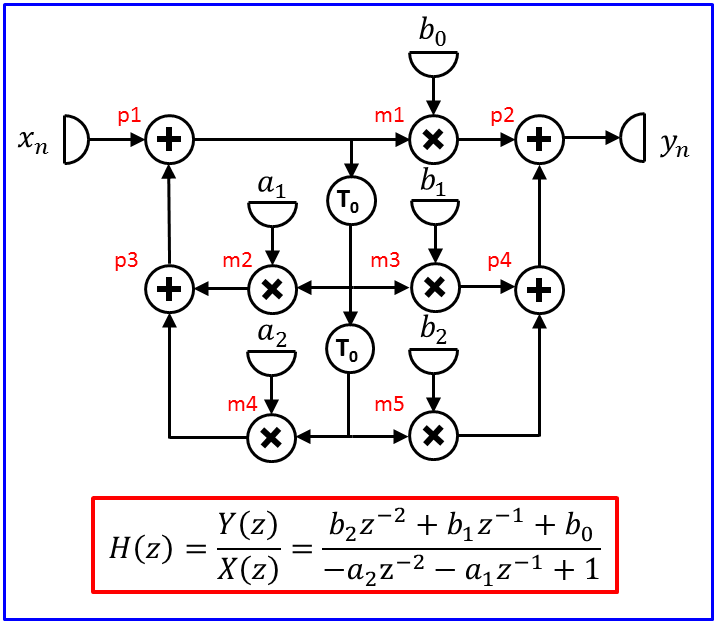

The additions in the DFG have been labeled with the letter p (of plus) followed by a digit. The multiplications have similarly been labeled with the letter m followed by a number. b0 to b2 and a1 to a2 are constants representing filter coefficients.
get-module map mapThree subdirectories of map will be created:
Run make (type make in the shell). You will see that for both Arx source files, C++ and VHDL will be generated. The warnings are related to the fact that the filter coefficients do not fit the given fixed-point data formats without loss of precision (you can ignore those warnings). For now, do not pay attention to the serial implementation.
cd ../cpp The source code for the C++ testbench consists of two files:
./tb_sec_df2.exe
The amplitudes of the two sinusoidal signals will be displayed. The following four output files will be created:
matlab
For the visualization of sec_df2_in_fixp.dat, type in Matlab:
load sec_df2_in_fixp.dat;
plot(sec_df2_in_fixp);
As mentioned, the testbench feeds the filter with a superposition of a low frequent and high-frequent sine wave. As the filter is a high-pass filter, the low-frequent signal should be strongly attenuated in the result. You can overrule the default amplitudes of 1.0 for the sines on the command line, using -l ⟨val⟩ for the amplitude of the low-frequent sine and -h ⟨val⟩ for the amplitude of the high-frequent sine. The following two commands disable the low-frequent input and respectively the high-frequent input:
./tb_sec_df2.exe -l0
./tb_sec_df2.exe -h0
Use visualization in Matlab (or any other program of your choice, such as MS Office Excel) to illustrate that the filter is indeed a high-pass filter.
What are the values of the first 5 output samples when simulating with both amplitudes being equal to one (default setting)?
cd ../vhdl
Launch Questasim and create a new project to which you add the following files to be compiled in the given order:
Trace relevant waveforms from Questasim and include them in your report. What are the values of the first 5 output samples that you see in Questasim? How do they compare to the samples of the C++ simulation? Explain possible differences.
Hint: To view variables in Questasim, you should enable (the check mark should be set) the Locals entry under the View menu. Then, when descending the design hierarchy, you should select the VHDL process in which the variable is declared. The variable will show up in the Locals window. You can then drag it to the Wave window.
Use the Linux diff command to compare the contents of output file sec_df2_out_vhdl.dat to the output stream of the corresponding C++ simulation. There should not be any difference.
If everything went well, the conclusion of this exercise should be that the C++ and VHDL generated from Arx behave exactly the same. This also means that it is not necessary to simulate the VHDL for each design made in Arx. The VHDL will serve primarily as input for synthesis. In practice, it is also wise to perform a post-synthesis simulation, but this is outside the scope of this course.
Then, a non-overlapped schedule using 11 clock cycles can be as follows:
time:   0   1   2   3   4   5   6   7   8   9   10
   *:   m4  m4  m2  m2  m5  m5  m3  m3  m1  m1  -
   +:   -   -   -   -   p3  p1  -   -   p4  -   p2
Completing the design, requires that the entire data path is specified, including registers, multiplexers, etc. Figure 12.19 of [Ger99] is the data path used for this design. It will not be reproduced here.
The register transfers below indicate for each computation the source and destination locations:
m1: ROM (b0), r1 -> r2    p1: i1, r4 -> d0, r1
m2: ROM (a1), d1 -> r3    p2: r2, r3 -> o1
m3: ROM (b1), d1 -> r3    p3: r2, r3 -> r4
m4: ROM (a2), d2 -> r2    p4: r2, r3 -> r4
m5: ROM (b2), d2 -> r2
The registers hold values as shown below:
time:   0   1   2   3   4   5   6   7   8   9   10
   r1:                          p1  p1  p1
   r2:          m4  m4  m4      m5  m5  m5      m1
   r3:                  m2              m3
   r4:                      p3              p4  p4
   i1:      di  di  di  di  di
   o1:  p2@
   d0:                          p1  p1  p1  p1  p1
   d1:  d0@ d0@ d0@ d0@ d0@ d0@ d0@ d0@ d0@ d0@ d0@
   d2:  d1@ d1@ d1@ d1@ d1@ d1@

di = data_in
The diagram shows the clock cycle when a value is written by using the label of the computation which produces that value until the clock cycle when the value needs to be kept. The @ sign indicates a value belonging to the previous iteration. Note that register r1 is redundant as it duplicates the contents of d0; d0 and d2 could be merged into a single register as the lifetimes of their contents do not conflict.
The C++ and VHDL for this model were already generated when make was called earlier. The simulation of this model is controlled by line:
#define CLOCKS_PER_SAMPLE 11
in file tb_sec_nov.cpp which will result in the run method to be called 11 times per input sample (see file tb_sec_generic.cpp).
Run the simulation and compare the output to the results of the parallel version of the filter.
Directory vhdl contains the generate-design script that you know from the System-on-Chip Design course. Use it to synthesize both the parallel and serial versions of the filter (do not forget to run it via srun). Note that the use of two clock cycles for a multiplication in the serial design is currently not specified in the synthesis script.
For each design, study the log file and pay special attention to the resource report. It mentions all adders and multipliers to be implemented by Synopsys including word lengths (in the reference report on the other hand, not all adders and multipliers are mentioned as some of them are directly expanded into gates).
For each design explain the information given in the resource report. For each resource, point out from which part of the Arx code it originates.
Now check the areas reported for both designs. Which of the designs is larger? Explain.
The schedule will be non-overlapping. Replace the delay elements by input-output pairs. How long (in clock cycles) is the critical path? Copy the DFG into your report and illustrate the critical path in the copied graph.
Draw the inequality graph for the DFG and use it to compute the mobility of each vertex in the DFG. assuming that the graph will be executed with the shortest iteration period allowed by the critical path. Such a schedule is called rate optimal.
Find a scheduling and an assignment that executes the DFG in the shortest iteration period possible. Given the constraint that the solution should be rate optimal (time-constrained scheduling), aim at minimizing the hardware to implement the design. Illustrate your solution in the usual way: draw a diagram where clock cycles increase along the horizontal axis while the resources are shown along vertical axis; use the labels in the DFG to refer to each individual addition and multiplication.
Finish the design by adding registers and multiplexers to your design. Try to minimize these resources as well using circular-arc-graph coloring if applicable. For each value stored in a register, show when it is written and when it is read for the last time. Then, construct the circular-arc graph and find a minimal coloring for it. The optimal number of registers should follow from this coloring.
Use a diagram that spans multiple iterations to illustrate optimal number of registers should follow from this coloring. href="http://wwwhome.cs.utwente.nl/~gerezsh/sendfile/sendfile.php/idsp-transform-extra.pdf?sendfile=idsp-transform-extra.pdf">addendum slide on transformations contains an example of such a diagram that shows both functional units and registers; it only shows part of the design, though, and it lacks a time axis, (in units of system clock cycles). In [Ger99], Figures 12.17, 12.18 and 12.19 present the solution obtained for the DFG of Figure 12.15 (Figure 12.13). Illustrate your solution using similar tables and diagrams.
Once all details of the design have been fixed, describe the design in Arx. Create a new file for this purpose in directory arx. Modify the makefile in that directory to include your new design.
When the Arx code compiles without errors, you can simulate it. Add a .cpp file in the cpp directory to create a C++ testbench. Modify the makefile in that directory to have your new testbench compiled. You could also opt for simulating it in VHDL. In such a case, create a new configuration in the vhdl directory. Simulate and try to make the design to have exactly the same output stream as the two provided implementations. Illustrate the correctness of your design using waveforms (VCD obtained from C++ or from direct simulations in VHDL) which show essential things like the repeated schedule and the fact that all multiplications take two clock cycles. If simulating VHDL, you will need to display waveforms of variables for this purpose (see MAP-2 on how to display them).
When ready with the design, synthesize the VHDL and discuss the performance figures (area, resources, critical path).
Note: Feel free to iterate several times between the paper design and its counterpart in Arx until your scheduling diagrams and the simulated waveforms fully match (if you have the time).
What is the value of the minimal iteration period? You will need that value for computing the mobility of vertices, as well as a value for the schedule latency: choose 8 clock cycles for the latency.
When done with the design in Arx, consider all design alternatives that you have looked at (including the "df2" and "nov" versions). Which of these would you implement in a real-life situation? Motivate your answer. Involve the concept of time-area trade-off in your motivation.
vcd2wlf debug.vcd debug.wlfdebug.wlf can now be viewed in Questasim. Call vsim and then open debug.wlf (choose the "log" file type).
This only works when there is a single Arx design in your simulation! Otherwise debug.vcd will get corrupted.
arx2pdf <your file>.arxand get:
<your file>.pdf.This command will recognize the keywords of Arx and use appropriate syntax highlighting. There also exists a command to convert just any ASCII file. You can call it with:
any2pdf <your file>.<your extension>As long as the extension indicates a well-known format such as .c (for C) or .cpp (for C++), the format will use an appropriate syntax highlighting. When using any2pdf, the .arx extension is not recognized; instead, use arx2pdf for Arx files.
For Exercises involving Arx, supply the Arx code written by you, waveforms obtained from VHDL or C++ simulations (when applicable), Matlab plots, synthesis results, etc.
| Go (back) to | Sabih's Home Page. |