Project GFS: The GFSK Receiver
This project is a compulsory part of the examination for the
Implementation of Digital Signal Processing
course at the University of Twente. The goals of this
project are:
- To exercise in fixed-point optimizations.
- To apply various aspects of the course on a larger design
considering area, time and power trade-offs.
Preparation
Read the document
Some
Background on GFSK Modulation
carefully. It contains the theory and some practical remarks that you
will need in the rest of this project. Consult also the lecture slides
on GFSK modulation as presented as part of the CORDIC theory.
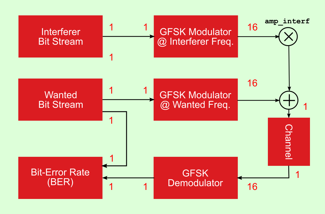
The GFSK system considered looks as follows:

As compared to the setup presented in the CORDIC lecture, the
system has two transmitters. The first is transmitting at the wanted carrier
(IF) frequency 1 MHz. The other is an interferer signal, for example
originating from a device operating in another radio channel; it
transmits at a frequency of 3 MHz. The wanted signal has an amplitude
of 1. The interferer has an amplitude amp_interf that can be
controlled by the testbench user. This amplitude is zero by default,
which amounts to the interferer not being present.
Interferers are quite common in radio communication. Many
standards have multiple channels in some frequency band. The systems
should be designed in such a way that communication in adjacent
channels should not interfere too much.
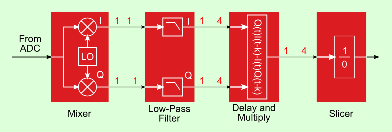
The system setup acts as testbench for the GFSK Demodulator, the
design of which is the topic of this project. As explained in the
background document, the demodulator is built from a chain of 4
signal-processing blocks, as follows:

Files and Directories
Go to your home directory and fetch the files for this project with:
get-module gfs gfs
Note: The first argument of get-module is the project
name, the second the name of subdirectory in your file system. So, by
issuing the command several times with a different second argument,
you will be able to make multiple copies of the distribution.
Three subdirectories of gfs will be created:
- arx: this subdirectory contains the source files in Arx
and the makefile for creating their C++ and VHDL models. Note
that each block in the demodulator chain is given by a separate Arx
file and needs to be compiled separately. It is up to the C++ and VHDL
testbenches to put the 4 Arx designs together.
- cpp: this directory contains the generated C++ files
along with the files that are used to build the C++ testbenches. They
are based on IT++.
- vhdl: this directory contains the generated VHDL files as
well as files to support synthesis and simulation.
A multitude of files are involved in this project. They will be
presented gradually, at the moment that they will be needed.
Change to subdirectory arx and run make. This
ensures that the database is consistent by generating the C++ and VHDL
versions of the Arx source files present in the subdirectory.
At this moment, you don't need to understand contents of the source
files.
Now change to directory cpp and run make in that
directory as well. You can ignore warnings originating from the IT++
source files.
The cpp directory has IT++ code for both the modulation
and demodulation as well as the C++ code corresponding to the four
demodulator blocks.
After running make 5 testbenches (5 compiled
executables) are created from a single generic source file
tb_ber.cpp:
- tb_ber_itpp: This testbench does not instantiate any Arx
blocks; the entire system is using IT++ models.
- tb_ber_mixer: This testbench instantiates the Arx
mixer and keeps the other IT++ models.
- tb_ber_filter: This testbench instantiates the Arx low-pass
filters next to the already instantiated mixer.
- tb_ber_demod: This testbench instantiates the
delay-and-multiply block from Arx next to the blocks already
instantiated in the previous testbench. It may be confusing, but the
term demodulator is used sometimes to refer to just the
delay-and-multiply block and sometimes to the entire chain from mixer
to slicer.
- tb_ber_slicer: This testbench uses Arx code for all four
blocks of the demodulator and is therefore the testbench to be used
for the final design. The other testbenches are useful for
intermediate versions of the design.
Each executable will perform a bit-error
rate (BER) simulation as follows.
The noise level is given by the signal-to-noise ratio (SNR).
The wanted signal has an amplitude of 1 and will not change throughout
the entire project (as opposed to a real-life situation where the
received signal can vary many orders of magnitude and gain
control in the analog front end keeps the signal in a relatively
small range). The SNR is computed with respect to that fixed wanted
signal level. So, SNR = 0dB amounts to having
as much signal power as noise power in the frequency band of interest.
In
a loop the SNR is gradually increased (the noise power is decreased)
in steps of 1 dB until the BER drops below
1.0e-4 (one error in 10.000 bits). At a specific SNR level,
the iteration is aborted
either when a maximum number of errors (1000) is
reached or a maximum number of bits have been simulated (100000).
If an SNR level is found with BER less than 1.0e-4, the
sensitivity level of BER = 1e-3 is estimated by interpolation.
Note: In this project description, the words bit and
symbol are used as equivalent notions as GFSK transmits one bit
per symbol.
As a sanity check, run all executables by typing the executable name
after the shell command prompt. Each simulation will display an SNR
level, the BER at that level, and between parentheses the number of
bits used for the computation of the BER.
If everything went well, all simulations will report a sensitivity level
of about 10.8 dB. Throughout the entire project this value will be
a reference for the quality of the design. Any design you make should
keep the sensitivity within 0.5 dB of this value, so below 11.3 dB.
The testbench executables all support the same command-line options:
- -d (dump mode, no arguments). This file will dump all
kind of intermediate data to file. Only use this option for a
limited number of bits (so in combination with option -b)
as you will create very large files otherwise.
- -s <float val> (SNR level). When specified, only one
SNR level is simulated. There will not be a search for the sensitivity
level.
- -b <int val> (number of bits). The simulation will
stop after the supplied number of bits (symbols) instead of the
default value of 100000.
- -o <int val> (slicer offset). This sets the
slicer-offset value necessary for a correct synchronization,
see also the background documentation. The supported values are 0, 1,
2 or 3.
Optimal values for all 5 testbench versions are built in after
being specified in file tb_ber.h.
- -p <int val> (symbol offset/pipeline depth). This
sets the number of symbols (bits) to be ignored at the beginning of
the simulation due to the latency in the system.
Optimal values for all 5 testbench versions are built in after
being specified in file tb_ber.h.
- -i <float val> (interferer amplitude). This controls
the value of amp_interf mentioned above.
Each of the 5 testbenches writes files in an output directory of
its own, named output_slicer, output_mixer, etc.
The following files are written:
- bits.err: This is the only file that is written without
the dump-mode option. It writes BER-SNR pairs and could be used to
plot the behavior of the BER vs. SNR.
- bits.in: This file contains the bits as transmitted in the
wanted channel.
- bits.out: This file contains the received bits.
- dam.out: The output of the DAM block, fixed-point
represented as floating point.
- lpf_i.out: The in-phase output of the low-pass
filter, fixed-point represented as floating point.
- lpf_q.out: The quadrature output of the low-pass
filter, fixed-point represented as floating point.
- mixer_i32.in: The mixer input (ADC output) in Arx integer
format, to be used as input for VHDL simulations (optional).
- mixer.in: The mixer input (ADC output) in fixed-point
format, represented as floating point numbers.
- mixer_i.out: The in-phase output of the mixer,
fixed-point represented as floating point.
- mixer_q.out: The quadrature output of the mixer,
fixed-point represented as floating point.
- mod.out: The modulator output, the received signal before
applying the quantization due to the ADC, fixed-point represented as
floating point.
- slc.out: The slicer output, the output bit stream
oversampled by a factor 4, where a 0 is represented by -1. Using -1
instead 0 may be of visual help when plotting the DAM output and
slicer output in the same graph.
Exercise GFS-1: Familiarization with GFSK
Study the background-information document in detail and try to match
it to the IT++ models of both transmitter and receiver as given in
files
gfsk.h,
gfsk.cpp,
tb_ber.h, and
tb_ber.cpp. The simulation operates bit by bit. For each bit,
the modulation function is called. Due to Gaussian filtering which
spans multiple bits (how many?),
the modulator needs to keep track of its history. Also at the
demodulator side, the simulation advances in steps of one bit and
history matters e.g. for the FIR filters.
Now run the following simulation (SNR = 100 dB basically means that
there is no noise):
tb_ber_itpp -d -b 1000 -s 100
Then, launch Matlab (command matlab) and in Matlab, plot the
frequency spectrum of the modulator output with:
load output_itpp/mod.out
periodogram(mod,[],2^13,8e6)
Inspect the spectra of intermediate signals working your way step by
step in the signal processing chain. Look at the ADC output, mixer
outputs and LPF outputs. Explain what you observe referring to the
theory.
Inspect the time signals dam.out and slc.out
as well as the input bit stream. Do you recognize
the input bit stream in the slicer output? How much latency does the system
have (how much "garbage" comes out of the slicer before the first
input bit is output)? How large is the amplitude of dam.out
and how does this relate to the theory presented in the background document?
Repeat the simulation with an interferer amplitude of 1.0. Comment
using the spectra as well as the time-domain plots.
Exercise GFS-2: Bit-Error Rate Simulations
As mentioned above, for bit-error-rate simulations, 100000 bits are
simulated by default and the sensitivity level is estimated in 4
decimals by simple interpolation. Investigate the accuracy of the
estimation by considering other orders of magnitude for the number of
bits (how are the values with 10000 or 1000000 bits?) and also by
making small variations around a given number (for example, 100001
or 100025 bits). What can you conclude about the accuracy? Is 100000 a
good number to simulate with for 4 (or maybe just 3) significant digits?
The correct synchronization is essential for the BER performance.
Two parameters that matter are the system latency, pipeline depth (for
the bits stored on behalf of BER calculations) or symbol
offset and the slicer offset. The optimal values for these
have been hard-coded in file tb_ber.h but can be overridden
with the -p and -o command-line options. For
testbenches tb_ber_itpp and tb_ber_slicer,
investigate neighboring values to the optimal settings. In some cases,
the BER will be degraded, in others the BER will collapse completely
and no sensitivity level will be found. Give a few examples of both
cases documenting the sensitivity numbers for each of the selected
settings.
The lesson learned is that synchronization is crucial for
performance. So, if you modify the design later on in a way that the
latency is affected, you will need to find the optimal offset values
again (inspecting the DAM and slicer outputs in the time domain may
give a good clue).
Exercise GFS-3: Arx Implementation of Demodulator
Inspect the Arx implementations of all four blocks in the demodulator
and compare them to their models in IT++. Describe the main
differences in a few sentences per block.
Perform the followng two simulations:
tb_ber_itpp -b 100 -s 100 -d
tb_ber_slicer -b 100 -s 100 -d
Plot the
dam.out signals of both simulations in one graph.
You should see two main differences. Mention and explain them.
For each Arx block estimate the number of flipflops used from the
source code. Report and motivate the numbers.
Exercise GFS-4: Demodulator in Arx: VHDL Synthesis
The distribution of this project comes with support for VHDL. An
entity gfsk.vhd is provided that instantiates all blocks
coming from Arx as well as a clock generator for the different clock
rates necessary. Word lengths are centrally administered in a file
pk_gfsk.vhd. The clock-generator is a "quick-and-dirty"
solution. In a real design, clock division would be implemented in a
more robust way (not relevant for this project).
A testbench is provided for a standalone VHDL simulation. You can
run a Questasim simulation if you are curious. As opposed to what you
are used, no configuration is provided as there is just one
architecture for each entity.
The compulsory part of
the VHDL work concerns synthesis. Synthesize the design using command
srun generate-design and inspect the log file when synthesis
is ready. The log file contains the size of each of the four blocks
in the demodulator as well information on its number of flipflops.
Create a table that shows for each block:
- its area,
- its number of flipflops,
- its average area per flipflop.
Is the number of flipflops a good indicator for the area of a block?
Exercise GFS-5: Fixed-Point Optimizations
Execute the following simulations:
tb_ber_itpp -i 7
tb_ber_itpp -i 10
You will observe that the BER performance behaves well at interferer
amplitude of 7 but not at 10. Now, edit file tb_ber.h and
increase the values for MIXER_WORD_LENGTH and
MIXER_IWORD_LENGTH by one. The values concerned are already
in the file and just need to be commented out. Recompile the
testbenches by running make and repeat the above simulations.
If everything went well, you should observe that the system can deal
with interferer amplitude 10.
This is, however, not true for the testbenches that incorporate Arx
designs.
Obviously, robustness against an
interferer was not taken into account when choosing the fixed-point
formats in the Arx code. A redesign action is needed.
In Arx, the fixed-point word lengths are provided in
Arx code. Go to the Arx directory and modify their fixed-point
parameters, making your way block by block from mixer to slicer and using the
appropriate testbench in the cpp directory. Optimize the
fixed-point parameters of each block and try to arrive in this way
(close) to the smallest design which
can deal with interferer amplitude 10. Each time you
modify Arx code, you will need to run make in the
arx and then the cpp directory. The goal is, of
course, not to make word lengths larger than necessary.
Summarize the results of all your experiments.
For each of the 4 blocks, present the observed
sensitivity for the fixed-point parameters that you have tried including the
parameter sets for which the sensitivity goal was no longer met.
Hints:
- The IT++ models are in floating point and are therefore much more
robust. Work on one Arx file at a time and use the appropriate
testbench to connect to the IT++ signal chain at the right point.
- To diagnose problems,
think of inspecting dumped signals
in the time and frequency domains. When relevant,
include plots in your report.
- Keep the parameters as used in IT++ consistent with the
generics used in Arx.
- Be aware that in the CORDIC implementation of the mixer, the
phase is a fixed-point number the length of which can be optimized.
When you have optimized all fixed-point parameters, go the
vhdl directory and synthesize the design. As you have changed
the word lengths, you will need to modify the values in file
pk_gfsk.vhd to reflect the changes before synthesis. Check
your log file for errors and warnings. If you are sufficiently
convinced that the synthesis was successful, make a new table with the
area and flipflop count per block, as you did for GFS-4.
Exercise GFS-6: Polyphase Implementation of the FIR Filters
The demodulator contains downsampling (by a factor 4) directly after
low-pass filtering. This means that a polyphase implementation,
exchanging the order of filtering and downsampling is possible (see
also the lecture slides).
Consider the advantages and disadvantages of a polyphase
implementation in this concrete case. You can involve the following
elements in your reasoning: one-to-one implementation vs. scheduled
solution, filter symmetry, multiplierless design, power-area-time
trade off. Do not write any code at this time. What is your final
recommendation regarding the polyphase implementation? Should it be
used or not?
Exercise GFS-7: Scheduled Solution
The reference design is a one-to-one implementation where the sample
frequency of 8 MHz is equal to the system clock frequency. Suppose
that the technology available to you allows a system clock of 80 MHz
and you can do arithmetic operations (add, multiply, etc.) in one
clock cycle.
Sketch on paper a data path, a bit in the style of Project MAP, that:
- can perform the entire GFSK reference design for the receiver;
- is flexible enough to execute alternative algorithms of comparable
complexity.
First estimate the
complexity of this design: how many additions, shifts,
multiplications, etc. would a data-flow graph of the entire receiver
have? How would those numbers translate in a minimum of
functional units (adders, multipliers, etc., FUs)? Involve the fixed-point
formats to determine the word lengths that the arithmetic blocks
should have.
By preference, the solution should look like the data path of a
single VLIW processor which can handle the entire demodulation.
Make use of
multi-ported register files from which FUs can read their
inputs and to which FUs can write their outputs. An extreme case of
such a multi-ported register file would allow all FUs to read and
write their data simultaneously from the same register file.
You do not need to be concerned with the controller. You can, for example,
assume that the controller is a sequencer that, for each clock cycle,
reads a pattern of control signals from an external memory (such a pattern can be considered
an "instruction"). This means
that the data path can be "programmed" by changing the contents of
this external memory.
You do not need to provide all details. A rough sketch in combination
with a motivation of your design choices and design
dimensioning is sufficient.
Exercise GFS-8: Free Design Assignment
Make, depending on the time left, minor or major modifications to the
Arx code for the GFSK receiver.
Follow any of the suggestions below, a subset or a combination or just
do something completely different.
- Replace the CORDIC by a dedicated mixer for 1 MHz; this is a
simple modification which has the disadvantage of sacrificing the
ability to compensate for variations in IF.
- Investigate alternatives for the implementation of the FIR filter:
transposed form instead of direct form, the use of multiplier blocks
(see reference [Lan02] on the main web page of this course),
etc.
- Consider a polyphase implementation in combination with hardware
sharing for the
I and Q channels (a polyphase implementation will reduce the clock
speed used in the filter by 4; if the clock is then doubled, the
computations for the I and Q channels can be done on the same hardware
in an interleaved fashion).
- Implement (part of) the architecture that you have proposed in
Exercise GFS-7.
As mentioned earlier, the constraint on your design should be to
keep the BER performance degradation
within 0.5 dB with respect to the original design.
Be aware that changing the number of registers in the
signal path may affect the system latency. If this is the case in your
design, you will need to find the optimal synchronization parameters.
You may need to modify the C++ testbench files. Try to keep
modifications to a minimum and make sure that Arx blocks are directly
connected to each other, so without performing intermediate
computations in the testbench.
Once your design is ready, run synthesis in order to have an
impression of the area and timing. You may synthesize the entire
receiver, but you may also consider synthesizing each component
separately.
For debugging Arx using generated C++, consult the debug "points of
attention" mentioned in the description of Project MAP.
As a last resort, you could try to debug the generated VHDL.
Deliverables
Write a short report always motivating your choices and explaining the
way you have reached your answers. Particular points of attention:
- GFS-1: Short explanation of modulator and demodulator,
illustrative plots from Matlab, answers to the
questions in the text.
- GFS-2: Results of BER simulations.
- GFS-3: Answers to the questions, requested plot, requested
numbers.
- GFS-4: The requested table on the synthesis results and your
comments.
- GFS-5: All new fixed-point values supported by plots and
BER simulation results. The table with synthesis results.
- GFS-6: The requested reasoning.
- GFS-7: The architecture that you have designed at the level of
detail that answers the questions and a motivation of your design
choices.
- GFS-8: A motivated presentation of your design, block diagrams,
Arx code, C++ testbench code (only if modified),
performance figures (both BER as well as speed and area after
synthesis), evaluation of the obtained improvement.
Grading
- GFS-1: 8 points
- GFS-2: 2 points
- GFS-3: 5 points
- GFS-4: 2 points
- GFS-5: 5 points
- GFS-6: 3 points
- GFS-7: 5 points
- GFS-8: 30 points (the number of points will depend on the
correctness and sophistication of your solution; as a reference, the
"dedicated mixer" solution, which is rather simple, will limit your
number of points to 15).
Last update on:
Fri Mar 15 16:40:09 CET 2024
by Sabih Gerez.
