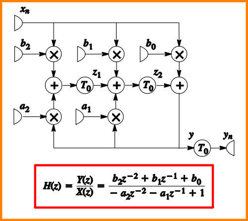
This project uses two sets of files to be stored in two different directories.
get-module sec syn
to get the first set of files in a subdirectory syn (assuming syn is the name of the directory you used for project SYN).
If one wants to deal with fractional numbers, one can agree to have an imaginary binary point in the bit vector. The number of bits at the right of the binary point determines the accuracy of the number system. With one bit, the accuracy is 1/2, with two it is 1/4 etc. (compare with the decimal notation system where the first position after the decimal point indicates 1/10, the second 1/100, etc.). The bits left of the binary point are called the integer bits and those at its right the fractional bits. For n fractional bits, the fractional number is obtained by dividing with a factor of 2 to the power of n with respect to the 2's-complement representation.
So a 5-bit vector with 3 integer and 2 fractional bits, can represent all numbers between -4 ("100.00") and +15/4 ("011.11") in steps of 1/4. If all 5 bits were fractional, the represented range would be from -1/2 (".10000") to +15/32 (".01111") in steps of 1/32.
A number with an associated binary point at some position is called a fixed-point number. An alternative way to deal with fractional numbers is to use floating-point numbers where part of the bit vector is a fraction and the other part an exponent with which the fraction should be scaled. Floating point numbers are not considered here any further as they need complex hardware for their implementation. The type of fixed-point number presented here is the signed variant. Also an unsigned variant exists.
The hardware needed for fixed-point numbers also differs somewhat from hardware for integer arithmetic. Additions of numbers with unequal positions of the binary point, for example, require that the binary points are aligned before adding them. In multiplications, the position of the binary point in the result depends on the binary-point positions of the two operands.
Special VHDL packages exist to represent fixed-point numbers. They are not used in this exercise. Instead, the signed data type is used and issues related to the fixed-point representation (especially when multiplying) are handled by explicitly coding them in VHDL.

The filter will be implemented as a new architecture for entity siso_gen. During the first 5 clock cycles after reset, the system will load the coefficients. After the 5th clock cycle, the input stream will be interpreted as data and the corresponding filtered output stream will be produced.
The computations in the filter are done by means of fixed-point arithmetic. In order to keep things simple, all signals have the same data type: two integer bits and word_length - 2 fractional bits where word_length is the generic parameter of the siso_gen entity. No distinction is made between the word lengths of data and coefficients, as opposed to real-life implementations.
The coefficients given in the first five positions of sec.in implement a high-pass filter. The data stream which follows, consists of three parts:
A reference output sec.ref contains the expected output. You can verify the correctness of your implementation by comparing the generated output file sec.out with sec.ref (use e.g. the Unix diff command to compare files).
A useful feature of Modelsim is to display a bit vector as an "analog" signal (see the manual). Make use of this feature. You should be able to e.g. see the sine shapes.
get-module nio nio
to get the files for this project in a subdirectory nio. You can also use this command to recover files that you lost for some reason or the other.
In the HDL-Based SoC Design module Qsys itself will not be used. Instead, a "frozen" design created by Qsys will be the basis for the exercises. The focus will be on the peripheral gp_custom for which you will design alternative architectures.
NIOS II is 32-bit processor. The system used in this exercise has the following address space:
| Component |
Base address |
End address |
Size |
| On-chip RAM |
0x00010000 |
0x0001FFFF |
64 kByte |
| NIOS II debug unit |
0x00020800 |
0x00020FFF |
2 kByte |
| gp_custom |
0x00021000 |
0x000210FF |
256 bytes |
| JTAG UART |
0x00021100 |
0x00021107 |
8 bytes |
In a practical design, the JTAG UART is a UART peripheral mapped on the FPGA's JTAG controller. This controller is used to communicate with a PC. In the current exercise, the JTAG UART is mainly used as an output port to which characters generated from a print command in C-code is sent to. In simulation, the characters will be displayed in the Questasim transcript window.
In this exercise, the architecture simple for gp_custom is provided as a starting point for developing more complicated behavior. The simple architecture has the capability to copy 16 words of 16 bits data from the outside world (via the SISO interface) into its internal input buffer or to copy 16 words from its output buffer to the outside world. The NIOS II can read from the input buffer or write to the output buffer and can also initiate data transfers. As the data bus of the NIOS II has a width of 32 bits, two words of the internal buffer are combined for transfer.
Draw a block diagram of the testbench and the NIOS II system descending the hierarchy down to the components instantiated by the mentioned files. Mention the names and functions of the most relevant entities and signals. The diagram should also provide some insight in how the data travels through the system.
To which write addresses does gp_custom react? And to which read addresses? Answer these questions with a table that contains a row for each address and tells per row what happens when reading and writing.
Mention two methods to intentionally stop the simulation in the given VHDL framework (hardware description and testbench).
volatile unsigned int *IO_CUSTOM=(unsigned int *)GP_CUSTOM_0_BASE;
Then, IO_CUSTOM[0] will access the first address in the peripheral IO[1] the second address, etc.
The development environment for software is found in a subdirectory called my_software. The compilation from C code to the bit patterns in RAM has been automated by means of a makefile called Makefile. Such a file lists dependencies between files that are created from each other and the commands that take care of the transformations. You do not need to understand the makefile; you only need to declare the name of your C file, e.g. foo.c in one of the first lines of the file. Typing make at the Unix command prompt will compile the file. If no errors are found, the final result will be a file called foo.hex. In a VHDL configuration, the file foo.hex will be connected to the RAM model by means of a generic map.
Suppose that a C-program that you have written, does not behave as you want, you can modify it, run make and then restart your simulation in Modelsim without quitting. The new object code will be used in the next run.
Start Modelsim in the main directory nio and create a new project. When asked whether to use the system or the current version of modelsim.ini choose for current. Make sure that the resolution is set to 1ps in the .mpf belonging to the project. Add the files mentioned in Exercise NIO-3 to the project and compile them in the given order. The VHDL sources of NIOS II itself have been pre-compiled in a separate library made available to you. Which configuration should you simulate in order to execute the code in copy.hex?
Note: due to way that Altera Qsys has generated VHDL, you cannot simulate the configuration in the usual way. Instead issue the following command in the transcript window:
start_sim <configuration name>
Run the simulation. Inspect input file copy.in and output file copy.out. Comment.
In the simulation, monitor the signals of gp_custom. How many clock cycles are needed to transfer the 16 data words from file to the CPU, reverse their order, and transfer them back to file? Pay attention as well to the print statements in the code. How many clock cycles per character does the execution of the alt_putstr function need? (Hint: in the wave window, set the format for signal av_writedata to ASCII.)
Which VHDL configuration should you use to execute this program? The input file for the simulation is sec_soft.in and its output is collected in sec_soft.out. sec_soft.ref contains a reference output stream.
Simulate the filter. It takes longer than usual. For this reason, a short message is printed after each block. Verify that the output in sec_soft.out coincides with the one in sec_soft.ref. Use Modelsim's Wave window to estimate the average number of clock cycles needed to calculate one block of samples including data transfer to and from the testbench. Do all blocks need the same number of clock cycles? How many clock cycles are roughly needed for one filter sample? With how many clock cycles per multiplication does this correspond if all other computations in the filter can be neglected?
In subdirectory my_software, you will find a file sec_soft.s which contains the assembly code that is the result of the compilation. Rename this file to sec_soft.s-keep for the purpose of future comparison (use Unix command mv). Now, clear the directory giving command make clean and then edit Makefile to use compiler optimization -O3 (uncomment the appropriate line). This option instructs the compiler to spend more compilation time with the goal of generating a more efficient executable. Run make to compile the software with the new options.
Finally, re-simulate the filter in Modelsim. How many cycles are now roughly needed for one block? And for one multiplication? Do all blocks need approximately the same number of clock cycles? Comment on the results.
Perform a post-synthesis simulation using command (typed on a single line):
start_sim_post <configuration name> <SDF file name>
where the SDF file name is the file name as found in the synopsys_out directory. Example:
start_sim_post conf_tb_nios_siso_copy_post gp_custom_simple_none_5_flat.sdf
assuming that your configuration and SDF files have the names used in the example.
Try to improve the performance of the execution of the second-order filter by modifying both the hardware as the software. Present a single solution, no multiple variants. This implies creating both a new architecture for the entity gp_custom and a new C-program. Use the VHDL configuration mechanism to simulate the new hardware-software combination. The co-processing hardware should have 2 integer and 8 fractional bits.
Think carefully about the software/hardware partitioning and try to find a good trade-off between speeding up the given software for the filter and keeping the hardware flexible. Flexibility amounts to creating hardware that can compute other things than just the given filter. It may be e.g. also an idea to have programmable filter coefficients. You are free to present any solution as long as you only modify the gp_custom architecture and software and leave all other hardware as is. The recommended solution is to extend gp_custom with only a multiplier (for numbers with two integer and 8 fractional bits) or a multiply-accumulate unit and let NIOS II send the operands and fetch the result.
Simulate your solution, and check that the output file is identical to the reference file. If you are satisfied with your design, synthesize gp_custom and perform a post-synthesis simulation.
Use the Canvas "file upload" feature to upload the following items (one upload per team):
| Go (back) to | Sabih's Home Page. |