The Dialmemo Chip
Most of the theoretical and practical concepts in the
ASIC Design Laboratory
are illustrated by means of the vehicle system called
the dialmemo. Besides, the dialmemo is actually designed by the
students down to the gate level. The idea to use this system for teaching
ASIC design originates from the Technical
University of Delft. However, the teaching material has been developed
almost entirely by the local staff in Twente.

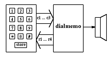
As can be seen from the picture above, the dialmemo is a device that
interacts with a telephone keyboard on one side and generates a sound signal
at the other side that can be reproduced by a loudspeaker. The user can
compose a telephone number on the keyboard and press the "*" key to activate
the production of tones that correspond with the number. Keeping the loudspeaker
against a telephone microphone should result in the number being dialed.
The dialmemo also has the possibility of storing a second "hidden" number
(using the "store" key which in practice may be less visible than on the
keyboard in the picture) and generate the tones associated with that
number using the "#" key. The dialmemo is a gadget that a company could
give away to its clients (the hidden number can then be used for the company's
own number).
Due to time constraints, the students are given the first level partitioning
of the system into the following entities:
-
an entity to scan the keyboard by sending out signals on the row wires
and observing the signals received on the column wires;
-
an entity that processes the detected keys and takes care of storage and
control;
-
an entity that generates the tones by digitally producing approximations
of sine waves of appropriate frequencies that are later converted to
analog signals by means of D/A converters.
After some 7 preparatory sessions of 4 hours each in which the students
become familiar with VHDL itself, its use in simulation and synthesis,
and perform some system-level design of the D/A converters as well,
students design the dialmemo by means of VHDL synthesis
in 5 more sessions.
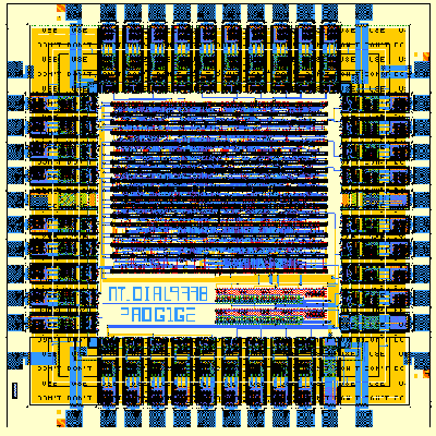
Below the layout of the chip designed by students
in the fall of 1997 and taped out by Hans Snijders
is shown. For the actual fabrication, the services of
Europractice
have been used. The experienced reader should see that the realization
uses standard cells except for the D/A converters on the lower right.

The
packaged chips function correctly and are currently used for the testing
sessions of the
ASIC Design Laboratory. In the newest
editions of the laboratory, student designs are directly mapped on a
demonstrator containing an FPGA.
Last update on:
Sun Jan 28 00:03:21 CET 2018
by Sabih
Gerez.
