 .
.
It is assumed that the student has completed project POW on low-power design and power simulations before starting this project.
The description below refers to various file names. Once you have logged in, execute the command:
get-module asy asy
to get them in a subdirectory asy, or copy them manually from the directory /home/practice/soc/exercise/modules/asy to directory asy (do not forget the "invisible" file .synopsys_dc.setup).
The design methodology used in this exercise differs from what you are used to. In order to be able to use a synchronous synthesis tool as the Synopsys Design Compiler, the design is partitioned into modules that are synthesized separately. The modules are then assembled to build the entire design. In this way, one can break feedback loops and one can avoid that logic cells in e.g. matched-delay lines are eliminated as a result of optimization. Note also that a tool like LEDA cannot be used for asynchronous designs (the existing rule set at least imposes a strictly synchronous design style).
The test-vector controller (TVC) can be found in file tvc_siso_asy.vhd. It has an internal clock which is not connected to the hardware. It is used to enforce a specific data rate such that comparisons of power consumption with synchronous equivalents of the design are possible. As it is complementary to the design under verification (DUV), the input channel is a push channel that reads data from file. In principle, first a reset pulse is generated and then data items from the input file are pushed into the DUV until the end of file is reached and the simulation is stopped. Request signals are synchronized with the internal clock. The output channel is passive and waits for request signals from the DUV. At each request the data is written to file and an acknowledge synchronized with the internal clock is generated. The TVC contains some time-out checks in order to stop the simulation when the DUV takes too long to react.
TVC and DUV are connected together in the testbench, as given in file tb_siso_asy.vhd. As in its synchronous counterpart, this setup has two hierarchical layers to make it possible that the generic word length can be set in a VHDL configuration.
The simplest DUV just connects its input channel to its output channel. The architecture of this feedthrough implementation of siso_asy can be found in file siso_asy_ft_arch.vhd. Compile entity and architecture for this design along with the TVC, testbench and the configuration given in file conf_ft.vhd. Simulate this design in order to become familiar with the setup. What is the time interval between data items at input and output?
The next DUV consists of a pipeline in the style of Figure 2.9 of the book by Sparsoe and Furber. A pipeline stage is given in the file pl_stage.vhd. It consists of two processes, one describing the Muller-C element taking care of the handshaking control and the other describing the latch with generic word length in the data path. By the way, when synthesized from this description, the Muller-C element will also be implemented by a latch. Note that latches are synthesized when if statements are used in which a signal is not assigned a value in all branches. Such constructs are typically qualified as wrong in synchronous designs. As opposed to earlier RTL-style code, signal assignments use a delay. These delays will be ignored by the synthesis tool but help in modelling asynchronous circuitry. Otherwise, the modelling of matched delays would become difficult.
A four-stage pipeline is built from pipeline-stage elements in siso_asy_pl4_arch.vhd. The description uses a VHDL construct that you may not yet know: the generate statement. It is used to instantiate subentities iteratively. In this way regular structures can be built. A generate statement can be preceded by a condition (this is not the case in this example) which is e.g. useful to instantiate different subentities along the borders of regular structures.
Compile the files pl_stage.vhd and siso_asy_pl4_arch.vhd as well as the configuration conf_pl4.vhd and simulate the 4-stage pipeline. Does the pipeline behave as a first-in first-out FIFO buffer? Explain what you see.
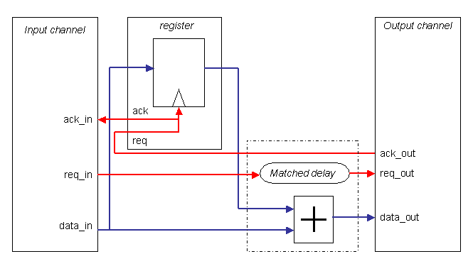
data_out(n) = data_in(n-1) + data_in(n)
It is implemented according to the schematics shown below where data signals are blue and handshaking control signals are red:
.
Compile the files just mentioned together with the configuration conf_add2.vhd and simulate. Verify that the circuit shows the intended behavior.
As mentioned earlier, the synthesis is done in small steps instead of reading all source files at once. The script syn-single is meant to synthesize a leaf component (a component at the lowest level of the hiearchy). You should not edit this script in principle, but only modify the file single-config to specify the synthesis parameters.
The provided version of single-config contains already the right set of parameters for the three leaf components et_register, adder and unit_delay. Synthesize them by commenting and uncommenting the appropriate lines and running syn-single. If everything goes well, each run produces a log file log_syn_single<run_id> and hierarchical and flattened versions of the design in VHDL and .db format. An SDF file is also written. As opposed to earlier exercises, the .db are essential and need to exist when assembling the design. Always check your log files to make sure that the synthesis went well.
The next step is to assemble the higher levels of the hiearchy. This is handled by the script syn-assemble and the associated configuration file assemble-config. The script reads the source files needed to build the entire hierarchy ending at the declared top-level entity, but does not synthesize. Instead, sublevels are replaced by instances of components that have already been synthesized. The variable MAP_LIST in the configuration script specifies the mapping. Once all components have been replaced by netlists (the script always uses the "flat" version), a log file, new hierarchical and flattened netlists and an SDF file are produced.
Use syn-assemble to assemble the matched delay and the gate-level description of the two-input pipelined adder. Important: when mapping one instance on another, the interface (inputs and outputs) should entirely match as well as the values assigned to the generics.
Study the log files obtained thus far. How long is the delay in the adder? How long is the delay in the matched delay? In order to avoid race conditions, one should dimension the matched delay with a 50 to 100 percent margin. Does this hold in this design?
Compile the gate-level netlist of add2 as well as the configuration conf_add2_gate.vhd and simulate. Do not forget the SDF file. Does the hardware perform correctly?
The scripts sim-gate and syn-gate that you know of the POW project are also available here. They make it possible to estimate the power consumed. Configuration is done from the file assemble-config.
Estimate the power consumed by add2 using stimuli from the file add2_random.in.
Now make a synchronous version of add2 in the directory that you have used for project POW. Make sure that you operate at the same data rate as the asynchronous circuit. First verify the functionality of your circuit interactively and then perform a power analysis. How does the power consumption compare to the asynchronous circuit? Comment on your results.
Note: The VHDL code provided for a Muller-C element and the pipeline stage are likely not to work after synthesis. If you run into too much trouble to make your post-synthesis simulation work, you may skip the synthesis and concentrate on pre-synthesis designs.
Suggestions for designs: