Project MAP: Mapping Data-Flow Graphs to RTL Designs
This project is a compulsory part of the examination for the
Implementation of Digital Signal Processing
course at the University of Twente. The goals of this
project are:
- To manually perform scheduling and assignment on a small design.
- To apply the theory of data-flow transformations to such a design.
- To learn the Arx language for modeling signal processing system at
the register-transfer level.
- To experiment with both the C++ and VHDL generated from Arx and
observe that their behavior is exactly equal.
- To actively design in Arx.
Preparation
This project assumes that you are familiar with:
- The Arx language as presented in the lectures. An on-line manual
of Arx is available at Bibix.
- Logic synthesis by means of Synopsys Design Compiler as was
performed in project
SYN
of the System-on-Chip Design course.
It is recommended that you
refresh your knowledge about the design flow: you should be able to
synthesize a given design and interpret the log files generated.
Performing post-synthesis simulations are less relevant
here.
The Filter
The figure below gives the data-flow graph (DFG) and z-domain description
of the filter to be used in this exercise.
The DFG represents the so-called
direct
form II of a second-order infinite impulse response (IIR)
filter, also called a digital biquad filter. It is actually
almost the same DFG as in Figure 12.13 of [Ger99] that you need to
study as part of the theory.
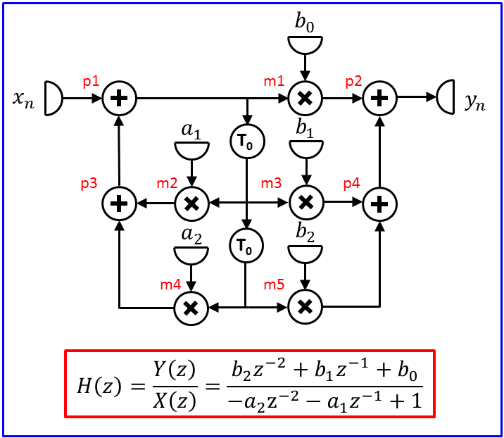
The additions in the DFG have been labeled with the letter
p (of plus) followed by a digit. The multiplications
have similarly been labeled with the letter m followed by a
number. b0 to b2 and a1 to a2 are
constants representing filter coefficients.
Exercise MAP-1: Rate-Optimal Non-Ovelapped Scheduling
Consider the implementation where adders need one clock cycle and
multipliers require
two clock cycles to compute their outputs. Both store their results in
a register (no chaining of computations).
The schedule will be non-overlapping. Replace the delay elements by
input-output pairs. How long (in clock cycles) is the critical path?
Copy the DFG into your report and illustrate the critical path in the
copied graph.
Using the
principles of mobility-based scheduling, first compute the
mobility of each vertex in the DFG assuming that the graph will be
executed with the shortest iteration period allowed by the critical
path. Such a schedule is called rate optimal.
Find a scheduling and assignment that executes the DFG in the
shortest iteration period possible. Given the constraint that the
solution should be rate optimal (time-constrained scheduling),
aim at minimizing the hardware to implement the design.
Illustrate your solution in
the usual way: draw a diagram where clock cycles increase along the
horizontal axis while the resources are shown along vertical axis;
use the labels in the DFG to refer to each individual addition and
multiplication.
Finish the design by adding registers and multiplexers to your
design. Try to minimize these resources as well. For each value
stored in a register, show when it is written and when it is read for the
last time. Use a diagram that spans multiple iterations to illustrate
your solution. The addendum
slide on transformations contains an example of such a diagram that
shows both functional units and registers; it only shows part of the
design, though, and it lacks a time axis,
(in units of system clock cycles).
In [Ger99], Figures 2.17, 2.18 and 2.19 present the solution obtained
for the DFG of Figure 2.15 (Figure 2.13).
Illustrate your solution using similar tables and diagrams.
Exercise MAP-2: Pipelining and Retiming for Non-Overlapped Scheduling
Apply pipelining and/or retiming transformations to reduce the
critical path of the DFG. If you need more than one elementary
transformation, illustrate each transformation separately.
Exercise MAP-3 [Only for teams of three members]: Full Details of
Optimized Design
Create a design based on your solution of MAP-2, providing full
details in the same style as you did for MAP-1.
Exercise MAP-4: Rate-Optimal
Overlapped Scheduling
Repeat MAP-1 now aiming for a solution that allows overlapped scheduling.
What is the minimal iteration period? You will need that value
for computing the mobility of vertices, as well as a value for the
schedule latency: choose 8 clock cycles for the latency.
Exercise MAP-5: Unfolding with a Factor 2
Unfold the original DFG, as given in the beginning of this page, by a
factor of two. Do this in such a way that the topology of the original
filter can be recognized in the unfolded graph as drawn by you.
Assuming that a multiplication requires two clock cycles and an
addition one, comment on the effects of the transformation on the
critical path and the critical loop.
Exercise MAP-6 [Only for teams of three members]: Unfolding with a Factor 3
Repeat MAP-5, now for unfolding factor 3.
Exercise MAP-7: One-Step Look-Ahead Transformation
Apply a one-step look-ahead transformation to the original filter. Try
to preserve the topology of the DFG as much as possible.
Assuming that a multiplication requires two clock cycles and an
addition one, comment on the effects of the transformation on the
critical path and the critical loop.
Exercise MAP-8 [Only for teams of three members]: Two-Step Look-Ahead
Transformation
Repeat MAP-7, now for the look-ahead transformation applied twice.
Files and Directories
The exercises above were meant to be solved on paper. Those below
require work on the soc1 server.
Go to your home directory and fetch the files for this project with:
get-module map map
Three subdirectories of map will be created:
- arx: this subdirectory contains the source files in Arx
and the makefile for creating their C++ and VHDL models.
- cpp: this directory contains the generated C++ files
along with the source codes for IT++ testbenches.
- vhdl: this directory contains the generated VHDL files,
the source code for VHDL testbenches as
well as files to support synthesis.
Arx Source Files
Change to directory arx. This directory contains three files:
- sec_df2.arx: The direct-form II DFG of the
second-order IIR filter as presented above, considered as an RTL
design. This means that the DFG is translated in a 1-to-1 fashion into
an RTL design, assuming that the sample period is a single clock
period and that the delay elements of the DFG are the only registers.
Altough Arx is an RTL design language and not a dataflow-simulation
language, the coding style as used in this file allows the
simulation of DFGs for verification purposes. This implementation will
be referred to as the parallel implementation of the filter.
- sec_nov.arx: An implementation of the same filter using
one adder and one multiplier after non-overlapped scheduling for a
situation where the adder takes one clock cycle and the multiplier
two. This implementation will be called from now on the serial
implementation of the filter
as it executes multiplications sequentially and the additions as well.
- Makefile: the makefile that takes care of generating C++
and VHDL from the Arx code.
Run make (type make in the shell). You will see that
for both Arx source files, C++ and VHDL will be generated. The
warnings are related to the fact that the filter coefficients do not
fit the given fixed-point data formats without loss of precision. For
now, do not pay attention to the serial implementation.
Exercise MAP-9: Arx C++ Simulation
Go to directory cpp:
cd ../cpp
The source code for the C++ testbench consists of two files:
- tb_sec_generic.cpp: the generic part of the testbench
to be reused for all design variations. It simulates the design by
applying the superposition of a low-frequent and a high-frequent sinusoidal
input signals to the
filter. It saves input and output data streams to file.
- tb_sec_df2.cpp: the specific part of the testbench. It
only declares a few parameters that are design specific.
Compile the C++ models by running make in the cpp
directory. You can ignore warnings in the compilation of IT++ code.
If things went well, this will result in the construction of the
executable file tb_sec_df2.exe. Run it with:
./tb_sec_df2.exe
The amplitudes of the two sinusoidal signals will be displayed. The
following four output files will be created:
- sec_df2_in_fixp.dat: input data stream in the chosen
fixed-point format (fixed-point numbers represented in floating-point
notation).
- sec_df2_out_fixp.dat: output data stream in fixed-point
format.
- sec_df2_in_int.dat: input data stream using integers,
corresponding to the internal representation in Arx.
- sec_df2_out_int.dat: output data stream using integers
corresponding to the internal representation in Arx.
The easiest way to visualize the streams is by means of Matlab. Launch
Matlab from th command line with command:
matlab
For the visualization of sec_df2_in_fixp.dat, type in
Matlab:
load sec_df2_in_fixp.dat;
plot(sec_df2_in_fixp);
As mentioned, the
testbench feeds the filter with a superposition of a low frequent and
high-frequent sine wave. As the filter is a high-pass filter, the
low-frequent signal should be strongly attenuated in the result.
You can overrule the default amplitudes of 1.0 for the sines on the
command line, using -l ⟨val⟩ for the amplitude
of the low-frequent sine and
-h ⟨val⟩ for the amplitude
of the high-frequent sine. The following two commands disable the
low-frequent input and respectively the high-frequent input:
./tb_sec_df2.exe -l0
./tb_sec_df2.exe -h0
Use visualization in Matlab (or any other program of your choice, such
as MS Office Excel) to illustrate that the filter is indeed a
high-pass filter.
What are the values of the first 5 output samples when simulating
with both amplitudes being equal to one (default setting)?
Exercise MAP-10: Simulate and Compare the C++ and VHDL Generated by
Arx
Go to the vhdl directory:
cd ../vhdl
Launch Questasim and create a new project to which you add the
following files to be compiled in the given order:
- arx_numeric.vhd: file with Arx VHDL utilities.
- sec_df2.vhd: the hardware generated from the Arx source code.
- tb_sec.vhd: a generic testbench to be used for all alternative
implementations of the IIR filter.
- conf_tb_sec_df2.vhd: A configuration to simulate
implementation version sec_df2 of the IIR filter.
Simulate configuration conf_tb_sec_df2 of the filter.
NOTE: always simulate the configuration and not an
entity-architecture combination! The testbench will read
sec_in_vhdl.dat as the input data stream. This stream has
been obtained from the C++ simulation with default amplitude values.
Trace relevant waveforms from Questasim and include them in your
report. What are the values of the first 5 output samples that you see
in Questasim? How do they compare to the samples of the C++
simulation? Explain possible differences.
Use the Linux diff command to compare the contents of
output file sec_df2_out_vhdl.dat to the output stream of the
corresponding C++ simulation. There should not be any difference.
If everything went well, the conclusion of this exercise should be
that the C++ and VHDL generated from Arx behave exactly the same. This
also means that it is not necessary to simulate the VHDL for each
design made in Arx. The VHDL will serve primarily as input for
synthesis. In practice, it is also wise to perform a
post-synthesis simulation, but this is outside the scope of this course.
Exercise MAP-11: Simulating the Serial Implementation of the
Second-Order IIR Filter
Go back to the arx directory and study the description of
file sec_nov.arx. It contains a serial implementation of the
second-order IIR filter
using a single
multiplier and a single adder. The design is explained below.
The labels, m1, m2, p1, p2, etc.
as used in the figure at the beginning will be used below to refer to
each of the multiplications and additions in the DFG.
Then, a non-overlapped schedule using 11 clock cycles can be as
follows:
time:   0   1   2   3   4   5   6   7   8   9   10
   *:   m4  m4  m2  m2  m5  m5  m3  m3  m1  m1  -
   +:   -   -   -   -   p3  p1  -   -   p4  -   p2
Completing the design, requires that the entire data path is
specified, including registers, multiplexers, etc.
Figure 12.19 of [Ger99] is the data path used for this design. It
will not be reproduced here.
The register transfers below indicate for each computation the source
and destination locations:
m1: ROM (b0), r1 -> r2    p1: i1, r4 -> d0, r1
m2: ROM (a1), d1 -> r3    p2: r2, r3 -> o1
m3: ROM (b1), d1 -> r3    p3: r2, r3 -> r4
m4: ROM (a2), d2 -> r2    p4: r2, r3 -> r4
m5: ROM (b2), d2 -> r2
The registers hold values as shown below:
time:   0   1   2   3   4   5   6   7   8   9   10
   r1:                          p1  p1  p1
   r2:          m4  m4  m4      m5  m5  m5      m1
   r3:                  m2              m3
   r4:                      p3          p4  p4  p4
   i1:  data_in
   o1:  p2@
   d0:                          p1  p1  p1  p1  p1
   d1:  d0@ d0@ d0@ d0@ d0@ d0@ d0@ d0@ d0@ d0@ d0@
   d2:  d1@ d1@ d1@ d1@ d1@ d1@
The diagram shows the clock cycle when a value is written by using the
label of the computation which produces that value until the clock
cycle when the value needs to be kept. The @ sign indicates a value
belonging to the previous iteration. Note
that register r1 is redundant as it duplicates the contents of
d0; d0 and d2 could be merged into a single
register as the lifetimes of their contents do not conflict.
The C++ and VHDL for this model were already generated when
make was called earlier.
The simulation of this model is controlled by line:
#define CLOCKS_PER_SAMPLE 11
in file tb_sec_nov.cpp
which will result in the run method to be called 11 times
per input sample (see file tb_sec_generic.cpp).
Run the simulation and compare the output to the results of the
parallel version of the filter.
Exercise MAP-12: RTL Synthesis
In this exercise, both the parallel and serial versions of the design
will be synthesized. Which of the two designs do you expect to be
larger? Motivate your answer before actually performing the
synthesis.
Directory vhdl contains the generate-design script
that you know from the System-on-Chip Design course. Use it to
synthesize both the parallel and serial versions of the filter (do not
forget to run it via srun). Note that the use of two clock
cycles for a multiplication in the serial design is currently not
specified in the synthesis script.
For each design, study the log file and pay special attention to the
resource report. It mentions all adders and multipliers to be
implemented by Synopsys including word lengths
(in the reference report on the other
hand, not all adders and multipliers are mentioned as some of them are
directly expanded into gates).
For each design explain the information given in the resource
report. For each resource, point out from which part of the Arx code
it originates.
Now check the areas reported for both designs.
Which of the designs is larger? Explain.
Exercise MAP-13 RTL Alternative(s)
Take your design of Exercise MAP-1 and describe it in Arx.
Create a new file for this purpose in directory arx.
Modify the makefile in that
directory to include your new design.
When the Arx code compiles without errors, you can simulate it.
Add a .cpp file in
the cpp directory to create a C++ testbench.
Modify the makefile in that directory to have your new testbench
compiled. You could also opt for simulating it in VHDL. In such a
case, create a new configuration in the vhdl directory.
Simulate and try to make the design to have exactly the same output
stream as the two provided implementations. Illustrate the correctness
of your design using waveforms (VCD obtained from C++ or from direct
simulations in VHDL) which show essential things like the repeated
schedule and the fact that all multiplications take two clock cycles.
When ready with the design, synthesize the VHDL and discuss the
performance figures (area, resources, critical path).
Repeat the above for your design of MAP-4, and, if you are a team of 3
persons, also for MAP-3.
Arx Points of Attention
Deliverables
Write a short report always motivating your choices and explaining the
way you have reached your answers. Do not be verbose. In particular,
do not copy the entire project description in your report. On the
other hand, be as complete as possible providing details of your
solutions by means of diagrams, (data-flow) graphs, tables, etc.
For Exercises involving Arx, supply the Arx code written by you,
waveforms obtained from VHDL or C++ simulations (when applicable),
Matlab plots, synthesis results, etc.
Grading
The exercises inside square brackets should be performed by teams of
three members only.
- MAP-1 [+ MAP-3]: 6 points
- MAP-2: 2 points
- MAP-4: 4 points
- MAP-5 [+ MAP-6]: 4 points
- MAP-7 [+ MAP-8]: 4 points
- MAP-9: 2 points
- MAP-10: 2 points
- MAP-11: 2 points
- MAP-12: 4 points
- MAP-13: 10 points
Last update on:
Mon Mar 25 07:59:51 CET 2019
by Sabih Gerez.